Post-Silicon Semiconductor Institute
-
14
Developed proprietary quantum error correction technology beyond the world's leading quantum computing companies
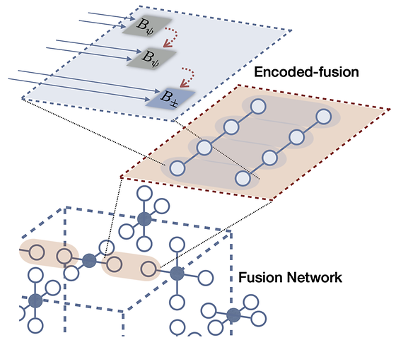
- Quantum error correction is a key technology in the implementation and practicalization of quantum computing - Groundbreaking quantum error correction technology contributes to the development of K-quantum computing deployments Solving the problem of error is essential for the practical application of quantum computing technologies that surpass the performance of digital computers. Information input into a qubit, the smallest unit of quantum computation, is quickly lost and error-prone. No matter how much we mitigate errors and improve the accuracy of qubit control, as the system size and computation scale increase, errors accumulate and algorithms become impossible to perform. Quantum error correction is a way to solve this problem. As the race for global supremacy in quantum technology intensifies, most major companies and research groups leading the development of quantum computing are now focusing on developing quantum error correction technology. Dr. Seung-Woo Lee and his team at the Quantum Technology Research Center at the Korea Institute of Science and Technology (KIST) have developed a world-class quantum error correction technology and designed a fault-tolerant quantum computing architecture based on it. They have demonstrated that this technology can outperform the quantum error correction technology recently developed by PsiQuantum, a global leader in the development of general-purpose quantum computers. The performance of universal quantum computing with quantum error correction is evaluated by its fault-tolerance threshold. This threshold indicates how well errors in quantum computing can be corrected, and the better the error correction technology and architectural design, the higher the value. PsiQuantum, an American quantum computer developer, has proposed a quantum computing architecture that utilizes photon entanglement resources, fusion techniques, and error correction technology, and is developing universal quantum computing hardware based on it. The photon loss threshold of the PsiQuantum method is reported to be 2.7%. The new error correction technique and quantum computing architecture developed by the KIST research team outperforms this. KIST's technology can achieve a photon loss threshold of up to 14%, which is currently the highest threshold in the world. In addition, KIST's error correction technique is much more resource-efficient than its quantum counterpart, even with the same photon consumption. The research is the first of its kind in Korea, and it is significant that Korea, a laggard in the field of quantum computing, has developed a world-class core technology. In particular, quantum error correction technology is an essential element in the development of quantum computers utilizing not only photon-based but also superconducting qubits, ion traps, and neutral atoms, which are highly competitive in R&D worldwide. This achievement shows that Korea has the potential to catch up with and even outpace the technology of leading countries in the quantum field. It is also expected to play an important role in building an independent quantum computing system by applying this achievement, which has completed domestic and international patent applications. "Just like semiconductor chip design technology, designing fault-tolerant architecture is important for quantum computing," said Dr. Seung-Woo Lee of KIST. Even if there are 1,000 physical qubits, it would be difficult to compute a single logical quantum task unless there is a structure that performs quantum error correction." 'The practicalization of quantum computing is still a long way off, but we believe that our research has contributed to bringing that time forward,' said Dr. Lee. [Figure 1] Fault-Tolerant Fusion-Based Quantum Computing Architecture with Quantum Error-Correcting Fusion / A fault-tolerant quantum computing architecture designed using quantum error-correcting encoded-fusion techniques. By adding layers of architecture, it utilizes multiple quantum error correction codes in fusion (Shor codes) and quantum computing architecture (Surface codes). [Figure 2] Photon Loss Tolerance Thresholds / Graph of photon loss tolerance threshold versus number of consumed photons compared to the results of PsiQuantum's method, Fusion-based Quantum Computing (FBQC). The encoded-fusion-based quantum computing (EFBQC) developed in this study achieves thresholds of up to 14%, significantly exceeding PsiQuantum's maximum threshold of 2.7%, and achieving significantly higher thresholds while consuming the same number of resources (photons). ### KIST was established in 1966 as the first government-funded research institute in Korea. KIST now strives to solve national and social challenges and secure growth engines through leading and innovative research. For more information, please visit KIST’s website at https://eng.kist.re.kr/ This research was supported by the Ministry of Science and ICT (Minister Yoo Sang-im) under the KIST Major Project and Bilateral Technology Cooperation Project (2022M3K4A1094774). The research was published* on August 1 in the international journal Physical Review Letters (IF: 8.1 JCR field top 6.8%).
- 13
- WriterDr. Seung-Woo, Lee
- 작성일2024.09.09
- Views1339
-
12
Enable distributed quantum sensors for simultaneous measurements in distant places
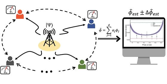
- Implementing a method for estimating spatially-distributed multiple parametersusing a small number of photons - Use quantum phenomena to enable distributed quantum sensors with precision beyond classical limits We've all had the experience of trying to get the exact time of a highly competitive concert ticket or class beforehand. If the time in Seoul and Busan is off by even a fraction of an hour, one will be less successful than the other. Sharing the exact time between distant locations is becoming increasingly important in all areas of our lives, including finance, telecommunications, security, and other fields that require improved accuracy and precision in sending and receiving data. The Korea Institute of Science and Technology (KIST) announced that Dr. Hyang-Tag Lim and his team at the Center for Quantum Information, in collaboration with leading domestic and international research institutes such as Chung-Ang University, the Korea Research Institute of Standards and Science (KRISS), the Agency for Defense Development (ADD), and the Oak Ridge National Laboratory (ORNL) in the United States, have succeeded in implementing a distributed quantum sensor that can measure multiple spatially-distributed physical quantities with high precision beyond the standard quantum limit with few resources. Quantum phenomena such as superposition and entanglement can be used to more precisely measure the time of different clocks in two distant spaces. Similarly, if you have two physical quantities, one in Seoul and one in Busan, you can share the entanglement state in Seoul and Busan and then measure the two physical quantities simultaneously with greater precision than if you measure the physical quantities in Seoul and Busan separately. There is an expectation that quantum sensors will enable ultra-precise measurements that are not possible with classical sensors, and 'distributed quantum sensors' are systems that can measure distributed multiple parameters over a large area with higher precision than conventional sensors. The KIST research team has experimentally demonstrated that distributed quantum sensing systems can be used to measure phenomena with the highest precision achievable with quantum mechanics in situations where the objects to be measured are distributed over a large area. The team experimentally generated a superposed maximum entanglement state that simultaneously exists in four spaces far apart from the Bell state, a quantum entanglement state, and applied it to reach the Heisenberg limit, the limit of quantum mechanical precision. "We look forward to expanding into practical technologies such as global time synchronization and ultra-microscopic cancer detection by pioneering the core source technology for distributed quantum sensing, which enables measurements beyond the standard quantum limit with few resources," said Dr. Hyang-Tag Lim of KIST, who led the study. KIST conducts open R&D projects to secure world-class source technologies in quantum applications, including quantum sensors, and disseminate them to industry, and is working with various researchers from industry, academia, and research centers, including first author Seongjin Hong, a professor at Chung-Ang University. [Fig 1] Distributed quantum sensing Send quantum states from a centralized location to each node distributed over a large area to obtain an average of the phases. ### KIST was established in 1966 as the first government-funded research institute in Korea. KIST now strives to solve national and social challenges and secure growth engines through leading and innovative research. For more information, please visit KIST’s website at https://eng.kist.re.kr/ This research, which was supported by the Ministry of Science and ICT (Minister Lee Jong-ho) through the KIST Major Project (2E32241) and the Information and Communication Technology Planning and Evaluation Institute (IITP) Quantum Sensor Core Strategic Technology Development Project (RS-2023-0022863), was published on January 11 in the international journal Nature Communications (IF: 16.6, JCR(%) 7.5). on January 11th. Journal : Nature Communications Title : Distributed quantum sensing of multiple phases with fewer photons Publication Date : 2024.01.11. DOI : https://doi.org/10.1038/s41467-023-44204-z
- 11
- WriterDr. Lim, Hyang-tag
- 작성일2024.02.06
- Views1032
-
10
Key LiDAR sensor elements for autonomous vehicles are now made with our technology
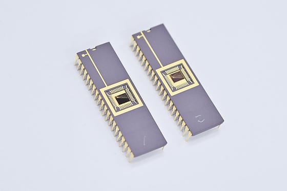
- High-performance sensor devices for short- and mid-range LiDAR applications - Expected to localize LiDAR sensor devices by developing based on a semiconductor mass production process LiDAR sensors are indispensable for the realization of advanced technologies such as advanced driver assistance systems (ADAS), autonomous driving, and AR/VR. In particular, short- and mid-range LiDAR used in AR/VR devices and smartphones requires better distance (depth) resolution to detect the shape of a person or object more accurately, and so a single-photon detector with better timing jitter performance is required. LiDAR measures distance and creates a 3D image by calculating the time it takes for a photon emitted by the transmitter to strike an object, reflect, and arrive back at the receiver. The slight difference in detection time that occurs when the single-photon detector at the receiver converts the light signal into an electrical signal is called "timing jitter," and the smaller the value of this jitter, the more accurately the object can be recognized. The Korea Institute of Science and Technology (KIST) announced that a team led by Dr. Myung-Jae Lee at the Post-Silicon Semiconductor Institute has developed a "single-photon avalanche diode (SPAD)" that can identify objects at the mm level based on a 40nm back-illuminated CMOS image sensor process. SPADs, which are ultra-high-performance sensor devices that can detect single photons, are extremely difficult to develop, and to date, only Sony of Japan has successfully commercialized SPAD-based LiDAR based on its 90nm back-illuminated CMOS image sensor process and supplied it to Apple products. Sony's SPAD shows better efficiency than back-illuminated SPADs reported in the literature, but its timing-jitter performance of about 137~222ps is insufficient to realize user discrimination, gesture recognition, and accurate shape recognition of objects required in short- and mid-range LiDAR applications. The single-photon sensor element developed by KIST has significantly improved the timing-jitter performance by more than two times to 56 ps, and the distance resolution has also been improved to about 8 mm, which has great potential for utilization as a short and mid-range LiDAR sensor element. In particular, since the SPAD was developed based on the 40nm back-illuminated CMOS image sensor process, a semiconductor process for mass production, through joint research with SK hynix, it is expected to be immediately localized and commercialized. "If commercialized as a core source technology for semiconductor LiDAR and 3D image sensors, it will greatly enhance our competitiveness in next-generation system semiconductors, which are Korea's strategic industries," said Myung-Jae Lee, principal investigator at KIST. [Fig 1] Simplified cross-section of a single-photon avalanche diode KIST single-photon avalanche diode developed in SK hynix's 40 nm back-illuminated CMOS image sensor technology [Fig 2] Semiconductor chip with ultra-high-performance sensor elements developed by Dr. Myung-Jae Lee's research team at KIST's Advanced Semiconductor Devices and Systems Laboratory (ADS Lab) [Fig 3] Dr. Myung-Jae Lee’s research team, Post-Silicon Semiconductor Institute, KIST (ADS Lab) ### KIST was established in 1966 as the first government-funded research institute in Korea. KIST now strives to solve national and social challenges and secure growth engines through leading and innovative research. For more information, please visit KIST’s website at https://eng.kist.re.kr/ The research, supported by the Korea Institute of Science and Technology (KIST) Institution Program (Grant No. 2E32242) and the National Research Foundation of Korea (NRF) (Grant No. 2021M3D1A2046731), was presented on December 12 at the International Electron Devices Meeting 2023 (IEDM 2023), held from December 9 to 13 in San Francisco, USA. IEDM is one of the most prestigious conferences for semiconductor industry and research experts, including major global semiconductor companies such as SK hynix, Samsung Electronics, and Intel.
- 9
- WriterDr. Lee, Myung-Jae
- 작성일2024.02.06
- Views1042
-
8
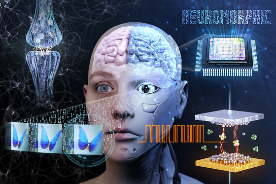
Implement artificial neural network hardware systems by stacking them like "neuron-synapse-neuron" structural blocks.
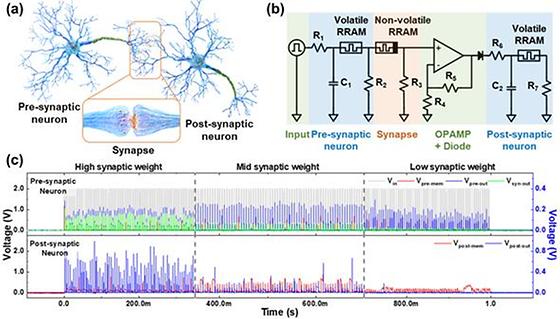
- Implementing the 'neuron-synapse-neuron' basic unit structure in hardware for high-performance, low-power neuromorphic computing - Same material, same structure for processability and network scalability With the emergence of new industries such as artificial intelligence, the Internet of Things, and machine learning, the world's leading companies are focusing on developing next-generation artificial intelligence semiconductors that can process vast amounts of data while consuming energy efficiently. Neuromorphic computing, inspired by the human brain, is one of them. As a result, devices that mimic biological neurons and synapses are being developed one after another based on emerging materials and structures, but research on integrating individual devices into a system to verify and optimize them is still lacking. In order for large-scale artificial neural network hardware to become practical in the future, it is essential to integrate artificial neuron and synaptic devices, and it is necessary to reduce mass production costs and energy usage by fabricating devices with the same materials and structures. A team led by Dr. Joon Young Kwak of the Center for Neuromorphic Engineering at the Korea Institute of Science and Technology (KIST) announced that they have implemented an integrated element technology for artificial neuromorphic devices that can connect neurons and synapses like "Lego blocks" to construct large-scale artificial neural network hardware. The team fabricated vertically stacked memristor devices using hBN, a two-dimensional material that is advantageous for high integration and ultra-low power implementation, to demonstrate biological neurons and synapses characteristics. Since the team designed artificial neuron and synaptic devices with the same material and the same structure, unlike conventional silicon CMOS-based artificial neural imitation devices with complex structures using multiple devices, the devices developed by the team have secured ease of process and network scalability, paving the way for the development of large-scale artificial neural network hardware. By integrating and connecting the developed devices, the team also successfully implemented the "neuron-synapse-neuron" structure, the basic unit block of an artificial neural network, in hardware to demonstrate spike signal-based information transmission, which is how the human brain works. By experimentally verifying that the modulation of spike signal information between two neurons can be adjusted according to the synaptic weights of the artificial synaptic device, the researchers showed the potential of using hBN-based emerging devices for low-power, large-scale AI hardware systems. "Artificial neural network hardware systems can be used to efficiently process vast amounts of data generated in real-life applications such as smart cities, healthcare, next-generation communications, weather forecasting, and autonomous vehicles," said KIST's Dr. Joon Young Kwak, explaining the significance of the research achievement. "It will help improve environmental issues such as carbon emissions by significantly reducing energy usage while exceeding the scaling limits of existing silicon CMOS-based devices." [Fig 1] Experimental results of modulating the connection strength of front and back neurons by synaptic weights. (a) Schematic diagram of a biological neural network and (b) circuit schematic of an artificial neural network implemented in hardware using an artificial neuromorphic device. (c) Experimental results of the change in connection strength between two neurons as the synaptic weight changes. It is observed that the degree of firing of the downstream neuron decreases as the synaptic weight decreases. [Fig 2] Two-dimensional material-based volatile and nonvolatile memory devices (a) Schematic representation of two-dimensional material-based volatile and non-volatile memory devices (top) and measured electrical properties of fabricated devices (bottom); (b) Electron micrographs (top) and transmission electron micrographs (bottom) of fabricated devices. Utilizing fabricated devices to emulate biological neuron and synapse properties. ### KIST was established in 1966 as the first government-funded research institute in Korea. KIST now strives to solve national and social challenges and secure growth engines through leading and innovative research. For more information, please visit KIST’s website at https://eng.kist.re.kr/ The research was funded by the Ministry of Science and ICT (Minister Jong-Ho Lee)'s Next Generation Intelligent Semiconductor Technology Development (Device) Project (2021M3F3A2A01037738) and KIST's Institutional Program and was published in the international journal Advanced Functional Materials (IF: 19.0, JCR(%): 4.2) online on November 5. Journal : Advanced Functional Materials Title : Hardware Implementation of Network Connectivity Relationships Using 2D hBN-Based Artificial Neuron and Synaptic Devices Publication Date : 2023.11.05. DOI : https://doi.org/10.1002/adfm.202309058
- 7
- WriterDr. Kwak, Joon Young
- 작성일2024.02.06
- Views1203
-
6
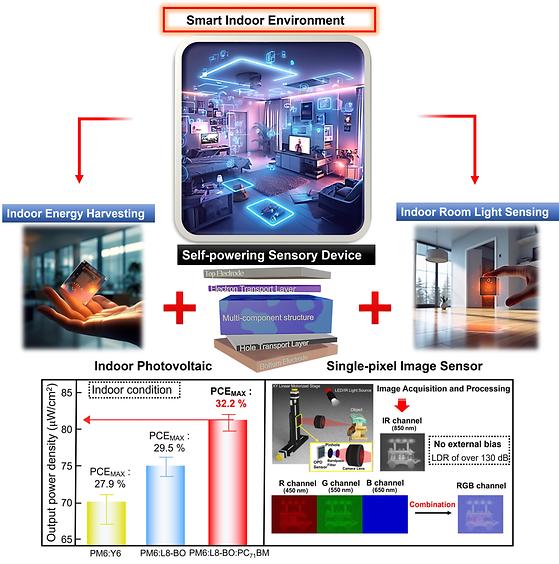
Advanced Full-color image sensor technology enabling simultaneous energy harvesting and imaging
- Single-pixel imaging successfully achieved for the first time using an organic-based photoelectric photodetector - Energy-efficient imaging in low-light conditions, facilitating human-computer interaction, shows promise for application in smart indoor environments Organic-based optoelectronic technology is increasingly recognized as an energy-efficient solution for low-power indoor electronics and wireless IoT sensors. This is largely due to its superior flexibility and light weight compared to conventional silicon-based devices. Notably, organic photovoltaic cells (OPVs) and organic photodetectors (OPDs) are leading examples in this field. OPVs have the remarkable ability to absorb energy and generate electricity even under very low light condition, while OPDs are capable of capturing images. However, despite their potential, the development of these devices has been conducted independently thus far. As a result, they have not yet reached the level of efficiency necessary to be considered practical for next-generation, miniaturized devices. The Korea Institute of Science and Technology (KIST), led by Dr. Min-Chul Park and Dr. Do Kyung Hwang of the Center for Opto-Electronic Materials and Devices, Prof. Jae Won Shim and Prof. Tae Geun Kim of the School of Electrical Engineering at Korea University, Prof. JaeHong Park of the Department of Chemistry and Nanoscience at Ewha Womans University, have developed an organic-based optoelcectronic device. This innovative device not only integrates the functionalities of organic photovoltaic cells (OPVs) and organic photodetectors (OPDs) but also pioneers in visualizing images in applications requiring low-light conditions, thereby enhancing energy efficiency in indoor environments. By advancing the organic semiconductor layer into a multicomponent structure, the research team has enhanced the device's performance. In door environments, it achieves an impressive photoelectric conversion efficiency exceeding 32%, along with a linear dynamic range surpassing 130 dB. This significant improvement in contrast ratio, especially in low-light conditions, allows for a much clearer image than conventional silicon devices, which typically offer a linear dynamic range of 100 dB. The collaborative research team made further strides by successfully applying single-pixel image sensing. This image sensing system capture ambient light, transforms into electrical energy, and utilize this energy to acquire images. In contrast to the previous need for specialized cameras in low-light of standard lighting conditions, the newly developed photodetector, featuring a multi-component semiconductor layer, offers a versatile application. It can function not only as a conventional camera but also as a decorative element on windows or walls, providing sufficient resolution to discern shapes and movements of objects. Dr. Min-chul Park from KIST highlighted the versatility of this technology, noting, "While primarily functioning as an energy harvester, it can also be applied to detect movement and recognize motion patterns in environments without light." He further expressed optimism about its potential applications, stating, "This holds great promise not only for human-computer interaction (HCI) research but also in various industrial sectors, including smart indoor environments." [Fig 1] Dual-function integrated image sensor Organics-based optoelectronic technology is gaining attention as an energy-efficient and environmentally friendly electronic device for Internet of Things (IoT)-based wireless sensors and low-power indoor electronics. Among them, organic photovoltaic (OPV) and organic photodetector (OPD) efficiently utilize ambient unutilized or low-light to generate electricity and detect light to implement images. Organic photovoltaics (OPVs) can be used to harvest indoor energy, while organic photodetectors (OPDs) can be used like cameras, utilizing indoor light for imaging as needed. ### KIST was established in 1966 as the first government-funded research institute in Korea. KIST now strives to solve national and social challenges and secure growth engines through leading and innovative research. For more information, please visit KIST’s website at https://eng.kist.re.kr/ This research was supported by the Ministry of Science and ICT (Minister Lee Jong-ho) as a KIST Institutional Program, a mid-career research support project of the Korea Research Foundation, and a Leader Research Project, and the results have been published in the international journal Advanced Materials (IF: 29.4, JCR(%): 2.312) and published online on November 2023. Journal : Advanced Materials Title : Self-Powering Sensory Device with Multi-Spectrum Image Realization for Smart Indoor Environments Publication Date : 2023.11.16. DOI : https://doi.org/10.1002/adma.202307523
- 5
- WriterDr. Park, Min-chul, Dr. Hwang, Do Kyung
- 작성일2024.02.05
- Views1056
-
4
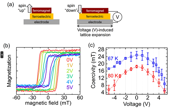
Quantum material-based spintronic devices operate at ultra-low power
- First development of spintronic device consisting of two-dimensional ferromagnetic-ferroelectric material heterostructure, observation of low-power voltage-driven device operation - Developed next-generation spin memory technology to secure technological advantage in the domestic semiconductor industry As artificial intelligence technologies such as Chat-GPT are utilized in various industries, the role of high-performance semiconductor devices for processing large amounts of information is becoming increasingly important. Among them, spin memory is attracting attention as a next-generation electronics technology because it is suitable for processing large amounts of information with lower power than silicon semiconductors that are currently mass-produced. Utilizing recently discovered quantum materials in spin memory is expected to dramatically improve performance by improving signal ratio and reducing power, but to achieve this, it is necessary to develop technologies to control the properties of quantum materials through electrical methods such as current and voltage. Dr. Jun Woo Choi of the Center for Spintroncs Research at the Korea Institute of Science and Technology (KIST) and Professor Se-Young Park of the Department of Physics at Soongsil University (President Beom-Sik Jang) have announced the results of a collaborative study showing that ultra-low-power memory can be fabricated from quantum materials. By applying a voltage to a quantum material spintronic device consisting of two-dimensional material heterostructure, it is possible to read and write information at ultra-low power by effectively controlling the spin information of electrons. Two-dimensional materials, which are representative quantum materials, can be easily separated into planar layers of single atoms, unlike ordinary materials that have a three-dimensional structure, and thus exhibit special quantum mechanical properties. In this study, we developed a two-dimensional heterostructure device that combines quantum materials with two different properties for the first time. By applying voltage as low as 5 V to a device consisting of a two-dimensional ferromagnetic material (Fe3-xGeTe2) and a two-dimensional ferroelectric material (In2Se3) stacked on top of each other, the magnetic field required to change the spin direction of the ferromagnet, i.e., the coercivity, can be reduced by more than 70%. The researchers also found that the structural changes in the two-dimensional ferroelectric that occur when a voltage is applied lead to changes in the spin properties of neighboring two-dimensional ferromagnets. The lattice of the two-dimensional ferroelectric expands with voltage, changing the magnetic anisotropy of the adjacent ferromagnet and greatly reducing the coercivity required to reorient the spin. This means that by applying a very small voltage to a quantum material heterostructure device, it is possible to control the spin information of electrons even with an approximately 70% reduced magnetic field, which is a key technology for the development of ultra-low-power spin memory based on quantum materials. "By securing ultra-low-power next-generation memory core element technology using quantum materials, we will be able to maintain our technological edge and competitiveness in the recently faltering semiconductor industry," said Dr. Jun Woo Choi of KIST. [Fig 1] Schematics and optical image of the two-dimensional(2D) material heterostructure device (a) Device schematics of two-dimensional(2D) ferromagnet-ferroelectric heterostructure device. (b) Optical image of the fabricated device. [Fig 2] Operation of the two-dimensional(2D) ferromagnet-ferroelectric heterostructure device (a) Operation scheme of the heterostructure device. Voltage-induced lattice expansion modulates the magnetic properties of the ferromagnet. (b) Voltage-dependent measurement of the magnetic properties. (c) The coercivity as a function of applied voltage. ### KIST was established in 1966 as the first government-funded research institute in Korea. KIST now strives to solve national and social challenges and secure growth engines through leading and innovative research. For more information, please visit KIST’s website at https://eng.kist.re.kr/ KIST Institutional Program (2E32251, 2E32252), Mid-Career Research Support Project (NRF-2021R1A2C2011007), Leading Research Center Support Project (NRF- 2020R1A5A1016518), and Nanomaterial Technology Development Project (NRF-2021M3H4A1A03054856) from the Ministry of Science and ICT (Minister Lee Jong-ho), (NRF-2021R1C1C1009494), and the National Research Foundation for Young Researchers (NRF-2021R1A6A1A03043957), this research was published in the international journal 「Nature Communications」. Journal : Nature Communications Title : Voltage control of magnetism in Fe3-xGeTe2/In2Se3 van der Waals ferromagnetic/ferroelectric heterostructures Publication Date : 2023.09.12. DOI : https://doi.org/10.1038/s41467-023-41382-8
- 3
- WriterDr. Choi, Jun Woo
- 작성일2024.02.05
- Views990
-
2
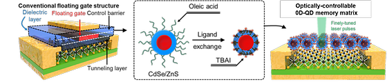
Ushering in the era of light-powered 'multi-level memories'
- KIST Developed technology to store and manipulate electronic states in quantum dots measuring 10 nanometers or less. We live in an era of data deluge. The data centers that are operated to store and process this flood of data use a lot of electricity, which has been called a major contributor to environmental pollution. To overcome this situation, polygonal computing systems with lower power consumption and higher computation speed are being researched, but they are not able to handle the huge demand for data processing because they operate with electrical signals, just like conventional binary computing systems. The Korea Institute of Science and Technology (KIST, President Seok Jin Yoon) announced that Dr. Do Kyung Hwang of the Center for Opto-Electronic Materials & Devices and Professor Jong-Soo Lee of the Department of Energy Science & Engineering at Daegu Gyeongbuk Institute of Science and Technology (DGIST, President Young Kuk) has jointly developed a new zero-dimensional and two-dimensional (2D-0D) semiconductor artificial junction material and observed the effect of a next-generation memory powered by light. Transmitting data between the computing and storage parts of a multi-level computer using light rather than electrical signals can dramatically increase processing speed. [Figure 1] 2D-0D HYBRID OPTICAL MEMORY DEVICES The research team has fabricated a new 2D-0D semiconductor artificial junction material by joining quantum dots in a core-shell structure with zinc sulfide (ZnS) on the surface of cadmium selenide (CdSe) and a molybdenum sulfide (MoS2) semiconductor. The new material enables the storage and manipulation of electronic states within quantum dots measuring 10 nm or less. When light is applied to the cadmium selenide core, a certain number of electrons flow out of the molybdenum sulfide semiconductor, trapping holes in the core and making it conductive. The electron state inside cadmium selenide is also quantized. Intermittent light pulses trap electrons in the electron band one after the other, inducing a change in the resistance of the molybdenum sulfide through the field effect, and the resistance changes in a cascading manner depending on the number of light pulses. This process makes it possible to divide and maintain more than 0 and 10 states, unlike conventional memory, which has only 0 and 1 states. The zinc sulfide shell also prevents charge leakage between neighboring quantum dots, allowing each single quantum dot to function as a memory. [Figure 2] Electron micrographs of the 2D-0D hybrid surface implemented in this study (top left), memory characteristics generated by light pulses (top right), and polynomial memory characteristics generated by multiple light pulses (bottom). While quantum dots in conventional 2D-0D semiconductor artificial junction structures simply amplify signals from light sensors, the team's quantum dot structure perfectly mimics the floating gate memory structure, confirming its potential for use as a next-generation optical memory. The researchers verified the effectiveness of the polynomial memory phenomenon with neural network modeling using the CIFAR-10 dataset and achieved a 91% recognition rate. Dr. Hwang of KIST said, "The new multi-level optical memory device will contribute to accelerating the industrialization of next-generation system technologies such as artificial intelligence systems, which have been difficult to commercialize due to technical limitations arising from the miniaturization and integration of existing silicon semiconductor devices." ### KIST was established in 1966 as the first government-funded research institute in Korea. KIST now strives to solve national and social challenges and secure growth engines through leading and innovative research. For more information, please visit KIST’s website at https://eng.kist.re.kr/ This research was supported by the Ministry of Science and ICT (Minister Jong-ho Lee) as a mid-career researcher project and a major project of KIST, and the results were published in the international journal Advanced Materials (IF: 29.4). Journal : Advanced Materials Title : Probing optical multi-level memory effects in single core-shell quantum dots and application through 2D-0D hybrid inverters Publication Date : 19-July-2023 DOI :https://doi.org/10.1002/adma.202303664
- 1
- WriterDr. Hwang, Do Kyung
- 작성일2023.10.17
- Views1324
-
0
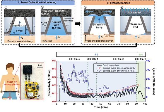
Development of a low-power, long-term sweat sensor patch that imitates sensory neurons
- Development of a sweat sensor patch that converts and processes sweat flow rate and ion concentration into spike signals - Resolves driving time and energy issues for long-term sweat monitoring unconventionally Human sweat contains chemical information including blood metabolites, ion concentrations, and nutrients. Monitoring this information using a wearable sensor can allow non-invasive (i.e. without blood sampling), real time health status tracking. For example, knowing sweat volume and ion concentrations can help people maintain adequate water and sodium levels during physical activities, and can prevent hypoglycemic shock by identifying symptomatic excessive sweating. Since a wearable sweat sensor patch generates a large amount of redundant data due to real-time continuous data wireless transmission and consumes a considerable amount of energy, it has been difficult to achieve sufficient operating time to render its use practical. Korea Institute of Science and Technology (KIST, President Seok Jin Yoon) announced that Dr. Hyunjung Yi's research team at the Center for Spintronics and professor Rhokyun Kwak's research team at the Hanyang University Department of Mechanical Engineering have developed a wearable sweat sensor patch with dramatically improved energy efficiency that can operate for more than 24 hours by imitating the efficient information processing method of sensory neurons. When a human sensory neuron receives external stimuli, it translates the information into spike signals. External stimulus strength is directly proportional to spike signal frequency. This event-based spike signal processing method used by neurons enables efficient, fast, and accurate processing of massive amounts of complex external stimulus data. If this "event-based wireless monitoring" method used by human sensory neurons is applied, data is only transmitted when important events related to the user's health indicators occur, minimizing energy consumption by the wireless monitor. These research teams have developed a wireless wearable sweat sensor patch that imitates the 'spike signals' of sensory neurons and has demonstrated in clinical trials the ability to dramatically reduce energy consumption through event-based wireless monitoring. Sweat is structured by the patch in a way that places a sweat removal layer on top of a conical open vertical sweat channel that can rapidly remove the sweat filling in the channel (Figure 2). Each sweat channel inner wall harbors a pair of electrodes, allowing conversion of the process of sweat filling the channel and getting removed into electrical signals. Electrical signals increase when channels are filled, and rapidly decrease each time the sweat is instantaneously removed. As this process is repeated, a spike-form signal is created. The frequency and amplitude of the spike signals carry interpretable information on the speed of sweat excretion and the concentration of sweat ion components. Through the repeated process of filling and emptying, the sweat sensor can operate continuously for a long period of time, and since newly secreted sweat is not mixed with preexisting sweat, the sensor can deliver accurate information. The research teams have experimentally proven that the energy consumption of this event-based data transmission method is only 0.63% of the energy consumption of continuous data transmission, allowing the developed wearable sweat sensor patch to operate continuously for more than 24 hours. Information from sweat on various skin surfaces in real exercise situations has successfully been obtained in clinical trials. Development of this patch enables long-term sweat monitoring that can be used to detect acute diseases or their precursors, such as nocturnal hypoglycemic shock and heart attack. The sensing method is expected to enable more energy-efficient and intelligent digital health management by application to other types of skin-attached sensors and adoption of new computing technologies. This research was conducted as a part of the Samsung Research Funding Center of Samsung Electronics and supported by a Midcareer Research Grant from the Ministry of Science and ICT (Minister Jong Ho Lee). It has been published as the Editors' highlight paper in the international journal 'Nature Communication'. Journal: Nature Communications Title: An epifluidic electronic patch with spiking sweat clearance for event-driven perspiration monitoring DIO: https://doi.org/10.1038/s41467-022-34442-y Schematic diagram of spike encoding in response to external stimuli by a biological sensory neuron and by the newly developed sweat sensor patch Structure and operating principle of the newly developed sweat sensor patch (top). Spike event-based wireless sweat monitoring clinical study using sweat sensor patch (bottom).
- -1
- Writer Dr. Yi, Hyunjung
- 작성일2023.02.16
- Views1263
-
-2
High-Performance and High-Reliability Artificial Synaptic Semiconductor Device Regarding Next-Generation Brain-Mimicking
- KIST discovered critical variables to maximize the performance of artificial synaptic devices - Green light for next-generation neuromorphic system development Neuromorphic computing system technology mimicking the human brain has emerged and overcome the limitation of excessive power consumption regarding the existing von Neumann computing method. A high-performance, analog artificial synapse device, capable of expressing various synapse connection strengths, is required to implement a semiconductor device that uses a brain information transmission method. This method uses signals transmitted between neurons when a neuron generates a spike signal. However, considering conventional resistance-variable memory devices widely used as artificial synapses, as the filament grows with varying resistance, the electric field increases, causing a feedback phenomenon, resulting in rapid filament growth. Therefore, it is challenging to implement considerable plasticity while maintaining analog (gradual) resistance variation concerning the filament type. The Korea Institute of Science and Technology (KIST, President Yoon Seok-jin), led by Dr. YeonJoo Jeong’s team at the Center for Neuromorphic Engineering, solved the limitations of analog synaptic characteristics, plasticity, and information preservation, which are chronic obstacles regarding memristors, neuromorphic semiconductor devices. He announced the development of an artificial synaptic semiconductor device capable of highly reliable neuromorphic computing. The KIST research team fine-tuned the redox properties of active electrode ions to solve small synaptic plasticity hindering the performance of existing neuromorphic semiconductor devices. Furthermore, various transition metals were doped and used in the synaptic device, controlling the reduction probability of active electrode ions. It was discovered that the high reduction probability of ions is a critical variable in the development of high-performance artificial synaptic devices. Therefore, a titanium transition metal, having a high ion reduction probability, was introduced by the research team into an existing artificial synaptic device. This maintains the synapse’s analog characteristics and the device plasticity at the synapse of the biological brain, approximately five times the difference between high and low resistances. Furthermore, they developed a high-performance neuromorphic semiconductor that is approximately 50 times more efficient. Additionally, due to the high alloy formation reaction concerning the doped titanium transition metal, the information retention increased up to 63 times compared with the existing artificial synaptic device. Furthermore, brain functions, including long-term potentiation and long-term depression, could be more precisely simulated. The team implemented an artificial neural network learning pattern using the developed artificial synaptic device and attempted artificial intelligence image recognition learning. As a result, the error rate was reduced by more than 60% compared with the existing artificial synaptic device; additionally, the handwriting image pattern (MNIST) recognition accuracy increased by more than 69%. The research team confirmed the feasibility of a high-performance neuromorphic computing system through this improved the artificial synaptic device. Dr. Jeong of KIST stated, “This study drastically improved the synaptic range of motion and information preservation, which were the greatest technical barriers of existing synaptic mimics.” “In the developed artificial synapse device, the device’s analog operation area to express the synapse’s various connection strengths has been maximized, so the performance of brain simulation-based artificial intelligence computing will be improved.” Additionally, he mentioned, “In the follow-up research, we will manufacture a neuromorphic semiconductor chip based on the developed artificial synapse device to realize a high-performance artificial intelligence system, thereby further enhancing competitiveness in the domestic system and artificial intelligence semiconductor field.” Image [Figure 1] Concept image of the article [Figure 2] Example of visual information processing technology using the artificial synaptic device, confirming that the error rate is reduced by more than 60% by improving the device performance [Figure 3] Photographs of (a) Solar Energy Collector, (b) Membrane Distillation System
- -3
- WriterDr. Jeong, YeonJoo
- 작성일2022.09.16
- Views1755
-
-4
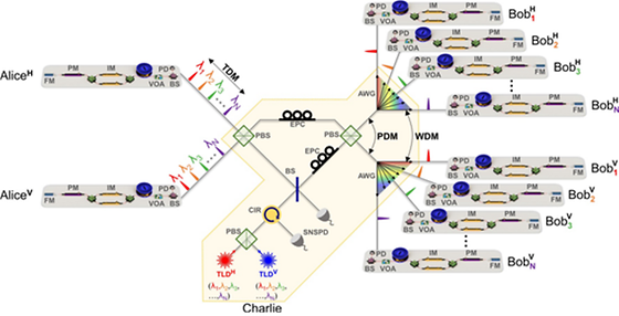
KIST develops key technology for quantum cryptography commercialization
- World’s second successful demonstration of Scalable TF QKD network structure In modern cryptosystems, users generate public and private keys that guarantee security based on computational complexity and use them to encrypt and decrypt information. However, recently, modern public-key cryptosystems have faced potential security loopholes against quantum computers with great computational power. As a solution, quantum cryptosystems have been highly noticed. They use quantum keys that guarantee security based on quantum physics rather than computational complexity, thus they are secure even against quantum computers. Therefore, quantum cryptosystems are expected to replace modern cryptosystems. Quantum key distribution (QKD) is the most important technology for realizing quantum cryptosystems. Two main technical issues should be addressed to commercialize QKD. One is the communication distance, and the other is the expansion from one-to-one (1:1) communication to one-to-many (1:N) or many-to-many (N:N) network communication. Twin-field (TF) QKD, announced in 2018, is a long-distance protocol, which can dramatically increase the communication distance of QKD systems. In TF QKD, two users can distribute a key by transmitting quantum signals to an intermediate third-party that is for measurement. Given the inevitable channel loss, this architecture allows the users to increase the communication distance. However, despite its innovativeness, it has been experimentally demonstrated by only a few global QKD leading groups owing to the significant difficulty of system implementation, and research on the TF QKD network is still insufficient. The Korea Institute of Science and Technology (KIST, Director Seok-jin Yoon) announced that their research team, the Center for Quantum Information, led by director Sang-Wook Han, succeeded in an experimental demonstration of a practical TF QKD network. This is the second experimental demonstration of the TF QKD network in the world after the University of Toronto in Canada. The research team proposed a new TF QKD network structure scalable to a two-to-many (2:N) network based on polarization-, time-, and wavelength-division multiplexing. Unlike the first demonstration of the University of Toronto based on a ring network structure, the research team's architecture is based on a star network. The quantum signal in a ring structure must pass through every user connected to the ring, however, the star structure only has it go through the center, making it possible to implement a more practical QKD system. Besides, to overcome the main implementation obstacles to developing the TF QKD system, the team applied a plug-and-play (PnP) structure. A conventional TF QKD system requires many control systems, such as timing, wavelength, phase, and polarization controllers, to maintain the indistinguishability of two quantum signals emitted by two users’ different light sources. Whereas in the PnP TF QKD architecture developed by the KIST research team, the middle third-party generates and transmits the initial signals to both users using a single light source, and the signals return to the third-party by making a round trip. Therefore, the polarization drift due to the birefringence effect of the channel is automatically compensated, and users have fundamentally the same wavelength. In addition, due to the two signals passing through the same route in opposite directions, the arrival times of the signals are naturally identical. As a result, only a phase controller is required for implementing the research team's architecture. Based on the architecture, the team successfully conducted an experimental demonstration of a TF QKD network. "It is a significant research achievement showing the possibility of solving the two main obstacles to QKD commercialization, and we have gained a key technology leading the corresponding research," said Sang-Wook Han, the leader of the Center for Quantum Information. - Image 2:N TF QKD network structure
- -5
- WriterDr. Han, Sang-Wook
- 작성일2022.07.23
- Views1705