Post-Silicon Semiconductor Institute
-
4
Malignant or benign? Quick and accurate diagnosis with artificial tactile neurons
- An artificial tactile neuron device that quickly and accurately converts the stiffness of a substance. - Combining with AI technology enables learning of the stiffness levels and distributions of the tumor, suggesting the possibility of cancer diagnosis. The stiffness levels and distributions of various biological materials reflect disease-related information, from cells to tissues. For example, malignant breast tumors are usually stiffer and have a more irregular shape than benign breast tumors. Ultrasound elastography can non-invasively determine the degree and shape of the tissue stiffness and is used for diagnosing breast cancer owing to its low cost. However, the opinion of an experienced expert is essential for interpreting ultrasound elastography images, but different experts differ in accuracy. The president of the Korea Institute of Science and Technology (KIST), Mr. Seok-Jin Yoon, announced that Dr. Hyunjung Yi's team at the spin convergence research center and Suyoun Lee, the director of the Center for Neuromorphic Engineering, had developed a simple but highly accurate disease diagnosis technology by combining tactile neuron devices with artificial neural network learning methods. Unlike the previously reported artificial tactile neuron devices, this tactile neuron device can determine the stiffness of objects. Neuromorphic technology is a research field that aims to emulate the human brain's information processing method, which is capable of high-level functions while consuming a small amount of energy using electronic circuits. Neuromorphic technology is gaining attention as a new data processing technology fit for AI, IoT, and autonomous driving, requiring the real-time processing of complex and vast information. Sensory neurons receive external stimuli through sensory receptors and convert them into electrical spike signals. Here, the generated spike pattern varies based on the external stimulus information. For example, higher stimulus intensity causes higher generated spike frequency. The research team developed an artificial tactile neuron device with a simple structure that combines a pressure sensor and an ovonic threshold switch device to produce such sensory neuron characteristics. Applying pressure to the pressure sensor causes the sensor's resistance to decrease and the connected ovonic switch element's spike frequency to change. The developed artificial tactile neuron device is a high-response, high-sensitivity device that allows the pressing force to generate faster electrical spikes while improving the pressure sensitivity, which focuses on the fact that stiffer materials result in faster pressure sensing when pressed. The electrical spike duration (or 1/frequency) generated by the developed device is less than 0.00001 s, which is more than 100,000 times faster than the several seconds it usually takes to press an object. Additionally, while the existing devices could detect a low pressure (approximately 20 kPa, similar to a force of light pressing) with a spike frequency change of 20 to 40 Hz, the developed device can detect the low pressure with spike frequency changes of 1.2 MHz. This allows real-time conversion of changes in the pressing force into spikes. To deploy the developed device to actual disease diagnosis, the research team used elastography images of malignant and benign breast tumors and utilized a spiking neural network learning method. Each pixel of the color-coded ultrasound elastography image which is correlated with the stiffness of the imaged material was converted into a spike frequency change value and used for training the AI. As a result, it was possible to determine the malignancy of a breast tumor with up to 95.8% accuracy. The KIST research team stated, "the developed artificial tactile neuron technology is capable of detecting and learning mechanical properties with a simple structure and method." The team added, "Through follow-up research, it will be possible to solve the noise reflection issue, which is a disadvantage of ultrasound elastography if artificial tactile neurons can collect an object's elastography image obtainable using ultrasound elastography." The team also expects the device to be helpful in low-power and high-accuracy disease diagnosis and applications such as robotic surgery where a surgical site needs to be quickly determined in an environment humans cannot directly contact." - Image The research results are published as an inside back cover paper in Advanced Materials.
- 3
- WriterDr. Yi, Hyunjung
- 작성일2022.07.09
- Views1404
-
2
A New Ultra-Thin Electrode Material: A Step Closer to Next-Generation Semiconductors
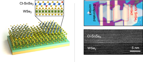
- Dramatically improved the performance of 2D semiconductor devices by supressing the Fermi-level pinning phenomenon - Expected to speed up the commercialization of next-generation system technologies such as miniaturization of artificial intelligence systems To realize artificial intelligence systems and autonomous driving systems, which is often seen in movies, in everyday life, processors that function as the brain of computers must be able to process more data. However, silicon-based logic devices, which are essential components of computer processors, have limitations in that processing costs and power consumption increase as miniaturization and integration progress. To overcome these limitations, studies are being conducted on electronic and logic devices based on very thin two-dimensional semiconductors at an atomic layer level. However, it is more difficult to control the electrical properties through doping in two-dimensional semiconductors than in conventional silicon-based semiconductor devices. Thus, it has been technically difficult to implement various logic devices with two-dimensional semiconductors. The Korea Institute of Science and Technology (KIST; President: Seok-jin Yoon) announced that a joint research team led by Dr. Do Kyung Hwang of the Center for Opto-Electronic Materials and Devices and Professor Kimoon Lee of the Department of Physics at Kunsan National University (President: Jang-ho Lee), has succeeded in implementing two-dimensional semiconductor-based electronic and logic devices, whose electrical properties can be freely controlled by developing a new ultra-thin electrode material (Cl-SnSe2). The joint research team was able to selectively control the electrical properties of semiconductor electronic devices using Cl-doped tin diselenide (Cl-SnSe2), a two-dimensional electrode material. It was difficult to implement complementary logic circuits with conventional two-dimensional semiconductor devices because they only exhibit the characteristics of either N-type or P-type devices due to the Fermi-level pinning phenomenon. In contrast, if the electrode material developed by the joint research team is used, it is possible to freely control the characteristics of the N-type and P-type devices by minimizing defects with the semiconductor interface. In other words, a single device performs the functions of both N-type and P-type devices. Hence, there is no need to manufacture the N-type and P-type devices separately. By using this device, the joint research team successfully implemented a high-performance, low-power, complementary logic circuit that can perform different logic operations such as NOR and NAND. Dr. Hwang said that, “this development will contribute to accelerating the commercialization of next-generation system technologies such as artificial intelligence systems, which have been difficult to use in practical applications due to technical limitations caused by the miniaturization and high integration of conventional silicon semiconductor devices." He also anticipated that "the developed two-dimensional electrode material is very thin; hence, they exhibit high light transmittance and flexibility. Therefore, they can be used for next-generation flexible and transparent semiconductor devices." Image Operation results of the two-dimensional semiconductor device and logic device implemented by the joint research team Structure of the two-dimensional semiconductor electronic device implemented in this study (left) and its image captured through an electron microscope (right)
- 1
- WriterDr. Hwang, Do Kyung
- 작성일2022.05.30
- Views1509
-
0
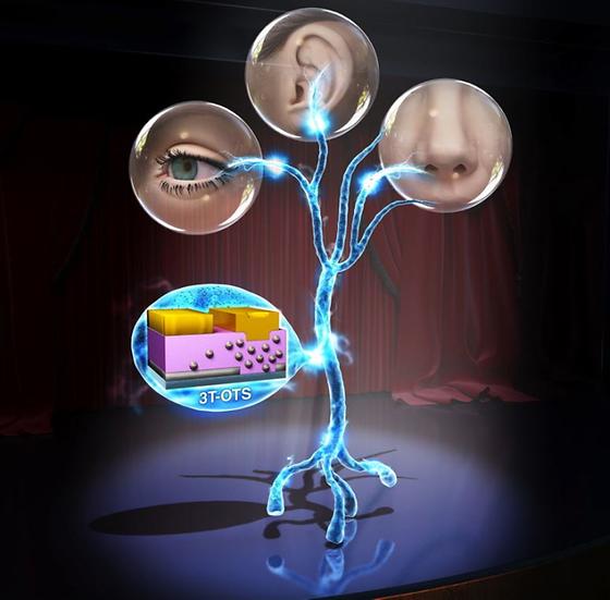
Development of low-power and high-efficiency artificial sensory neurons
- 3T-OTS device to simulate the efficient information processing method of the human brain - A green light for the development of sensor-AI combined next-generation artificial intelligence “to be used in life and safety fields” Currently, AI services spread rapidly in daily life and in all industries. These services are enabled by connecting AI centers and terminals such as mobile devices, PCs, etc. This method, however, increases the burden on the environment by consuming a lot of power not only to drive the AI ??system but also to transmit data. In times of war or disasters, it may become useless due to the power collapse and network failures, the consequences of which may be even more serious if it is an AI service in the life and safety field. As a next-generation artificial intelligence technology that can overcome these weaknesses, low-power and high-efficiency 'in-sensor computing' technology that mimics the information processing mechanism of the human nervous system is drawing attention. The Korea Institute of Science and Technology (KIST, President Seok-Jin Yoon) announced that its team led by Dr. Suyoun Lee (Center for Neuromorphic Engineering) has succeeded in developing ‘artificial sensory neurons’ that will be the key to the practical use of in-sensor computing. Neurons refine vast external stimuli (received by sensory organs such as eyes, nose, mouth, ears, and skin) into information in the form of spikes; and therefore, play an important role in enabling the brain to quickly integrate and perform complex tasks such as cognition, learning, reasoning, prediction, and judgment with little energy. The Ovonic threshold switch (OTS) is a two-terminal switching device that maintains a high resistance state (10-100 MΩ) below the switching voltage, and exhibits a sharp decrease in resistance above the switching voltage. In a precedent study, the team developed an artificial neuron device that mimics the action of neurons (integrate-and-fire) that generates a spike signal when the input signal exceeds a specific intensity. This study, furthermore, introduces a 3-terminal Ovonic Threshold Switch (3T-OTS) device that can control the switching voltage in order to simulate the behavior of neurons and quickly find and abstract patterns among vast amounts of data input to sensory organs. By connecting a sensor to the third electrode of the 3T-OTS device, which converts external stimuli into voltage, it was possible to realize a sensory neuron device that changes the spike patterns according to the external stimuli. The research team succeeded in realizing an artificial visual neuron device that mimics the information processing method of human sensory organs, by combining a 3T-OTS and a photodiode. In addition, by connecting an artificial visual neuron device with an artificial neural network that mimics the visual center of the brain, the team could distinguish COVID-19 infections from viral pneumonia with an accuracy of about 86.5% through image learning of chest X-rays. Dr Suyoun Lee, Director of the KIST Center for Neuromorphic Engineering, said, “This artificial sensory neuron device is a platform technology that can implement various sensory neuron devices such as sight and touch, by connecting with existing sensors. It is a crucial building block for in-sensor computing technology.” He also explained the significance of the research that “will make a great contribution to solving various social problems related to life and safety, such as, developing a medical imaging diagnostic system that can diagnose simultaneously with examinations, predicting acute heart disease through time-series pattern analysis of pulse and blood pressure, and realizing extrasensory ability to detect vibrations outside the audible frequency to prevent building collapse accidents, earthquakes, tsunamis, etc.”. Image Distinguishing COVID-19 infection through image learning of chest X-rays The 3T-OTS device provides a platform for developing artificial sensory neurons, which generate spikes responding to external stimuli.
- -1
- WriterDr. Lee, Suyoun
- 작성일2022.04.08
- Views1212
-
-2
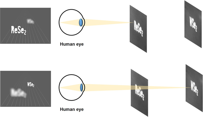
3D Digital Holograms on Smartphones?
Realized 3D digital holograms by developing a polarization image sensor with no additional polarization filters. Miniaturization of the entire holographic camera sensor module is possible with follow-up research 3D holograms, previously seen only in science fiction movies, may soon make their way into our daily lives. Until now, 3D holograms based on phase shifting holography method could be captured using a large, specialized camera with a polarizing filter. However, a Korean research group has just developed technology that can acquire holograms on mobile devices, such as smartphones. <p style="box-sizing: border-box; margin-top: 5px; margin-bottom: 15px; color: rgb(51, 51, 51); font-family: " open="" sans",="" "helvetica="" neue",="" helvetica,="" arial,="" sans-serif;="" font-size:="" 14px;="" background-color:="" rgb(255,="" 255,="" 255);="" line-height:="" 1.5;"="">The Korea Institute of Science and Technology (KIST, Director Seok-jin Yoon) recently announced that a research team led by Dr. Min-Chul Park and Dr. Do Kyung Hwang of the Center for Opto-Electronic Materials and Devices, in collaboration with a research team led by Prof. Seongil Im of the Department of Physics at Yonsei University, was successful in developing a photodiode that detects the polarization of light in the near-infrared region without additional polarization filters and thus, the realization of a miniaturized holographic image sensor for 3D digital holograms, using the 2D semiconductor materials: rhenium diselenide and tungsten diselenide. <p style="box-sizing: border-box; margin-top: 5px; margin-bottom: 15px; color: rgb(51, 51, 51); font-family: " open="" sans",="" "helvetica="" neue",="" helvetica,="" arial,="" sans-serif;="" font-size:="" 14px;="" background-color:="" rgb(255,="" 255,="" 255);="" line-height:="" 1.5;"=""> <p style="box-sizing: border-box; margin-top: 5px; margin-bottom: 15px; color: rgb(51, 51, 51); font-family: " open="" sans",="" "helvetica="" neue",="" helvetica,="" arial,="" sans-serif;="" font-size:="" 14px;="" background-color:="" rgb(255,="" 255,="" 255);="" line-height:="" 1.5;"="">Photodiodes, which convert light into current signals, are essential components within the pixels of image sensors in digital and smartphone cameras. Introducing the ability to sense the polarization of light to the image sensor of an ordinary camera provides a variety of new information, enabling the storage of 3D holograms. Previous polarization-sensing cameras have an additional polarization filter, several hundred micrometers in size, attached to an ultra-small optical diode image sensor, less than a micrometer in size. Thus, they could not be implemented into portable electronic devices because of their inability to be integrated and miniaturized. <p style="box-sizing: border-box; margin-top: 5px; margin-bottom: 15px; color: rgb(51, 51, 51); font-family: " open="" sans",="" "helvetica="" neue",="" helvetica,="" arial,="" sans-serif;="" font-size:="" 14px;="" background-color:="" rgb(255,="" 255,="" 255);="" line-height:="" 1.5;"=""> <p style="box-sizing: border-box; margin-top: 5px; margin-bottom: 15px; color: rgb(51, 51, 51); font-family: " open="" sans",="" "helvetica="" neue",="" helvetica,="" arial,="" sans-serif;="" font-size:="" 14px;="" background-color:="" rgb(255,="" 255,="" 255);="" line-height:="" 1.5;"="">The research group developed a photodiode by stacking an n-type semiconductor, rhenium diselenide, which exhibits a difference in light absorption dependent on the linear polarization angle of light in the near-infrared (980 nm) region, and a p-type semiconductor, tungsten diselenide, which exhibits no difference in photo-response dependent on polarization, but enables superior performance. The device is excellent in the photodetection of various wavelengths from ultraviolet to near-infrared, even capable of selectively detecting the polarization characteristics of light in the near-infrared region. The research group utilized the device to create a digital holographic image sensor that records polarization characteristics to successfully capture holograms. <p style="box-sizing: border-box; margin-top: 5px; margin-bottom: 15px; color: rgb(51, 51, 51); font-family: " open="" sans",="" "helvetica="" neue",="" helvetica,="" arial,="" sans-serif;="" font-size:="" 14px;="" background-color:="" rgb(255,="" 255,="" 255);="" line-height:="" 1.5;"=""> Dr. Hwang of KIST said, "Research on the downsizing and integration of individual elements is required to ultimately miniaturize holographic systems. The results of our research will lay the foundation for the future development of miniaturized holographic camera sensor modules." In addition, Dr. Park remarked, "The new sensor can further detect near-infrared light, as well as previously undetectable visible light, opening up new opportunities in various fields such as 3D night vision, self-driving, biotechnology, and near-infrared data acquisition for analyzing and restoring cultural assets." Image HOLOGRAM IMPLEMENTED WITH TWO-DIMENSIONAL SEMICONDUCTOR WSE2/RESE2, WHICH IS A POLARIZATION-SENSING PHOTODIODE, RESE2 ON THE FRONT AND WSE2 ON THE BACK ARE IMAGED IN THREE-DIMENSIONAL SPACE
- -3
- WriterDr. Min-Chul Park and Dr. Do Kyung Hwang
- 작성일2022.01.05
- Views2004